Chapter 8: I/O
I/O Basics
1. Device Registers
The simplest I/O devices usually have at least 2 device registers: one to hold the data being transferred between the device and the computer, one to hold the device status information, such as whether the device is available or it is processing the most recent I/O task.
2. Memory-Mapped I/O vs Special Input/Ouput Instructions
In the past, computers use special input and output instructions. Now, most computers use data movement instructions to handle I/O tasks. I/O device registers are mapped to a set of memory addresses that are allocated to I/O devices registers rather than memory locations.
The LC-3 uses memory-mapped I/O. Addresses xFE00 to xFFFF are reserved for I/O device registers. In particular, xFE00 and xFE02 are for KBSR and KBDR, and xFE04 and xFE06 are for DSR and DDR.
3. Asynchronous vs Synchronous
Most I/O devices operate at speeds different from that of the microprocessor, and not in lockstep. This characteristic is called asynchronous.
To control an asynchronous device requires a protocol or handshaking mechanism. We’ll need a single-bit register as the flag (Ready bit). As for the input device, the Ready bit is set when the typist types a character (and the computer is ready to start reading that character), and cleared when the computer finishes reading that character. As for the output device, the Ready bit is cleared when a character is shipped to the monitor, and set set when the monitor finishes processing that character (and the computer is ready to start sending another character).
4. Interrupt-Driven vs Polling
There are two ways for the computer to interact with the I/O device.
In interrupt-driven I/O, the I/O device controls the interaction. The processor does its own thing until being interrupted by the I/O device, pauses its current task, and handles the interrupt request.
In polling, the processor controls the interaction. The processor interrogates the Ready bit of the device status register again and again, until it detects that the Ready bit is set. Then it reads the device data register.
Polling
The Basic Input Service Routine
START     LDI   R1, KBSR
          BRzp  START      ; Test bit 15 of KBSR. If 0, wait
          LDI   R0, KBDR   ; Char read to R0
          BRnzp NEXT_TASK
KBSR      .FILL xFE00
KBDR      .FILL xFE02
NEXT_TASK
The Basic Output Service Routine
START     LDI   R1, DSR
          BRzp  START     ; Test bit 15 of DSR. If 0, wait
          STI   R0, DDR   ; Display char in R0
          BRnzp NEXT_TASK
DSR       .FILL xFE04
DDR       .FILL xFE06
NEXT_TASK
Keyboard Echo
START     LDI   R1, KBSR  ; Test input register ready
          BRzp  START
          LDI   R0, KBDR
ECHO      LDI   R1, DSR   ; Test output register ready
          BRzp  ECHO
          STI   R0, DDR
          BRnzp NEXT_TASK
KBSR      .FILL xFE00
KBDR      .FILL xFE02
DSR       .FILL xFE04
DDR       .FILL xFE06
NEXT_TASK
Implementation of Memory-Mapped I/O
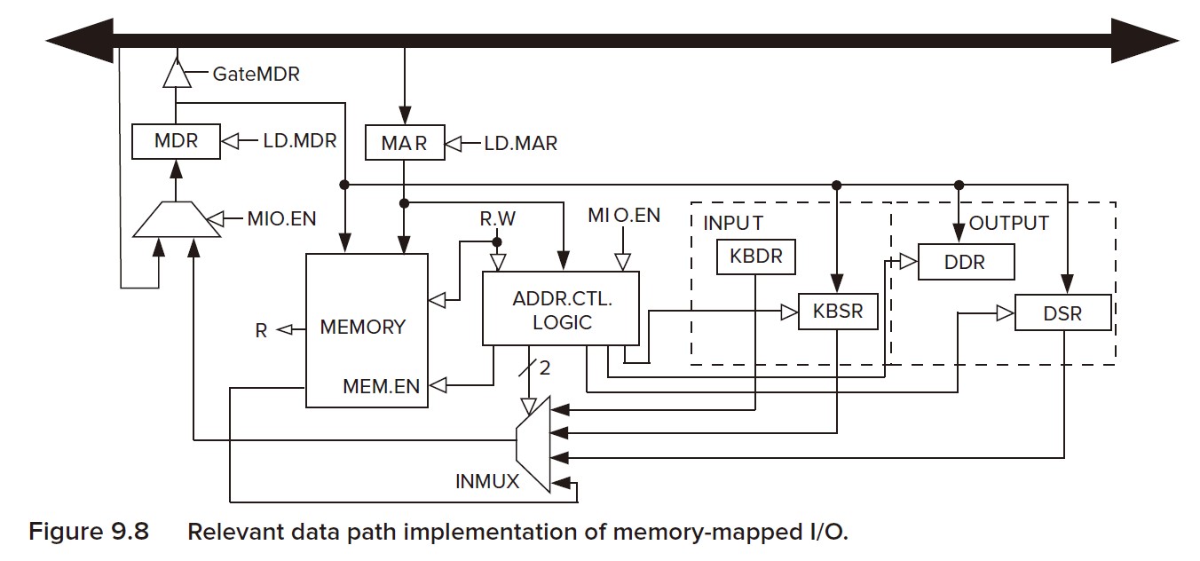
Above is the data path related to memory-mapped I/O. The Address Control Logic (ACL) block determines whether memory should be accessed or I/O device registers should be accessed. It is supplied with two signals, R.W (whether load or store is requested) and MIO.EN (whether memory or I/O is accessed), and the contents of MAR.
If the contents of MAR is a real memory location, the ACL outputs MEM.EN signal to enable memory, and provides select lines to INMUX to select memory.
If the contents of MAR is an address mapped to an I/O device, MEM.EN is not asserted. Meanwhile, if R.W indicates a load, The ACL provices select lines to INMUX to source the corresponding device register. If R.W indicates a store, the ACL asserts the load enable signal to the device register specified by the contents of MAR.