

Chapter 3: Digital Logic Structures
The transistors
- n-type transistor: if the gate is supplied with 1, it’s conductive, otherwise unconductive.
- p-type transistor: if the gate is supplied with 0, it’s conductive, otherwise unconductive.
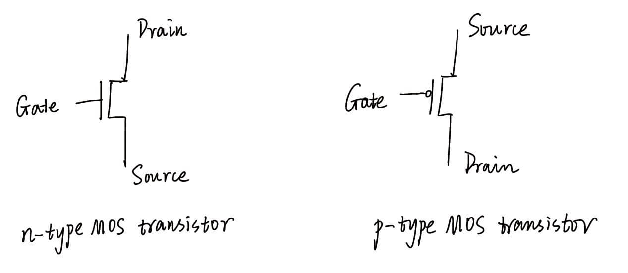
Threshold voltage drop: An n-type transistor with an input 1 behaves like a piece of wire only when connected to GND. If it is connected to +, there is a transmission voltage of approx. 0.5 volts across the transistor.
Similarly, An p-type transistor with an input 0 behaves like a piece of wire only when connnected to +. If it is connected to GND, there is a transmission voltage of approx. 0.5 volts across the transistor.
Thus, in normal use, n-type transistors are connected to GND, while p-types are connected to +.
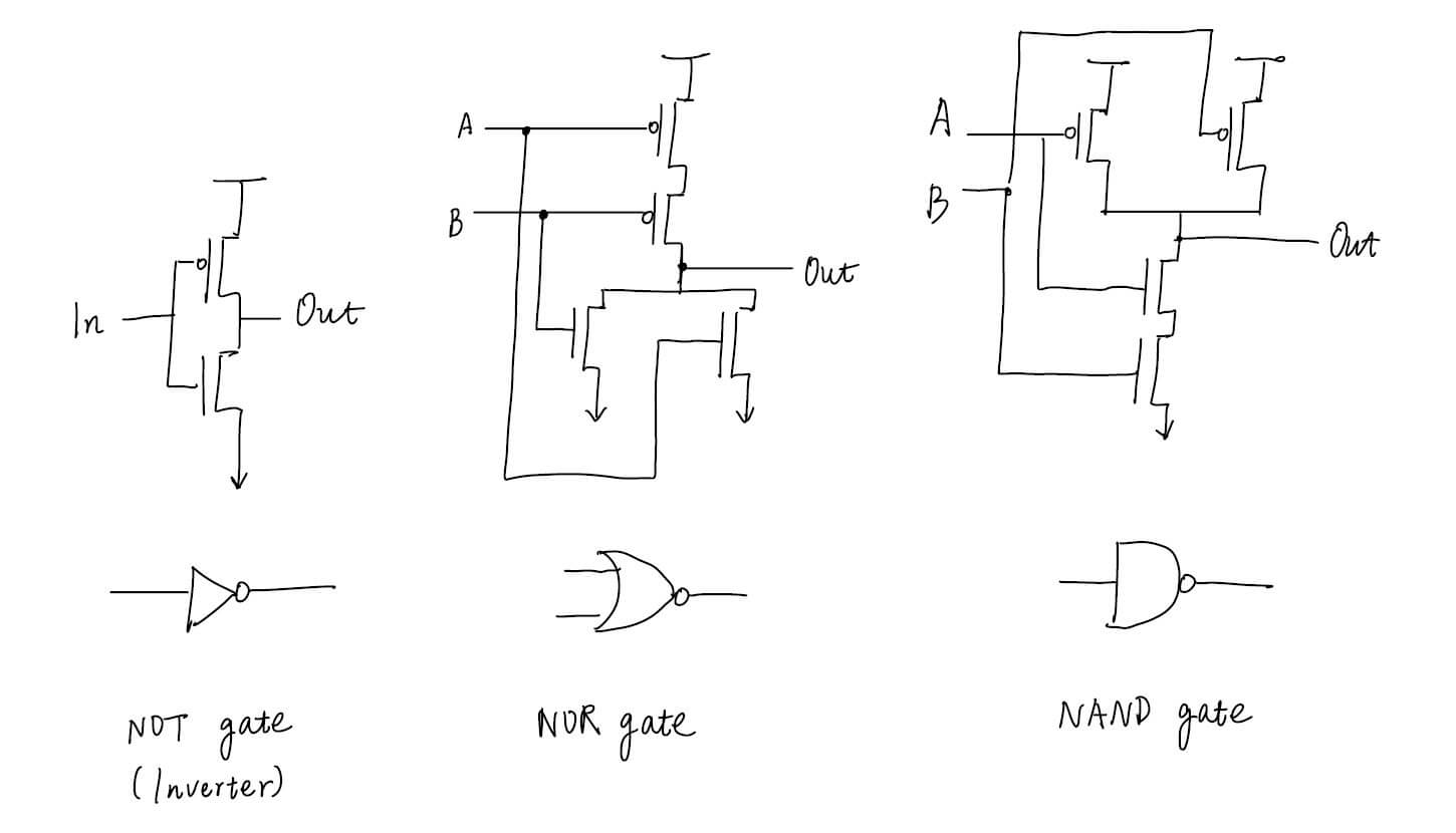
Logic Gates
NOT, NOR and NAND Gates
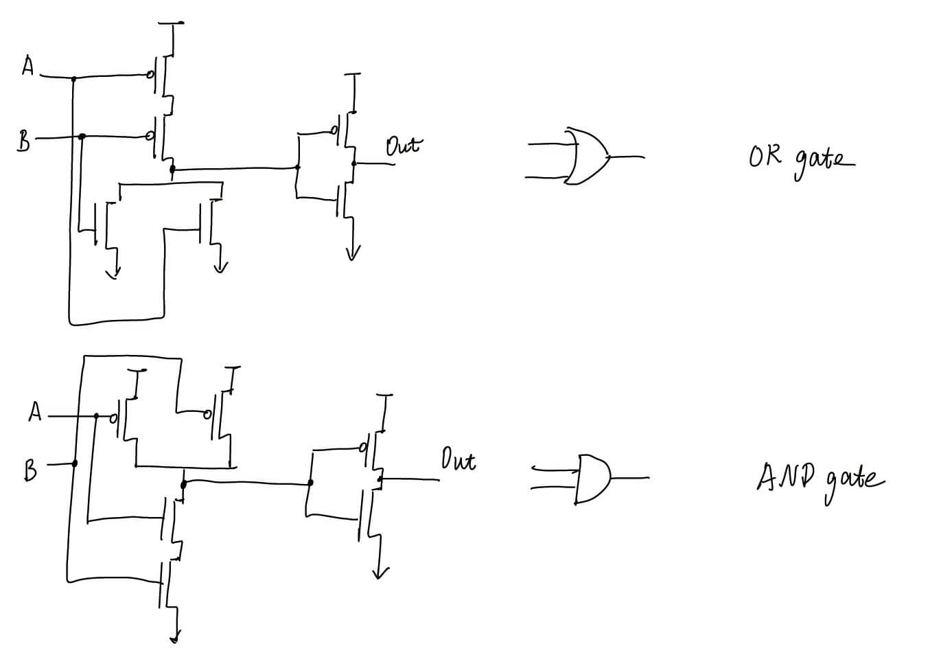
OR and AND Gates
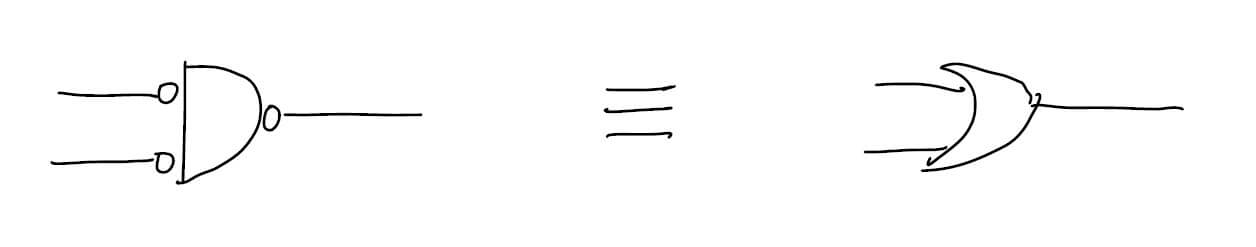
De Morgan’s Law
Combinational Logic Circuits
These logic circuits do not store information. The output is entirely dependent on the current input.
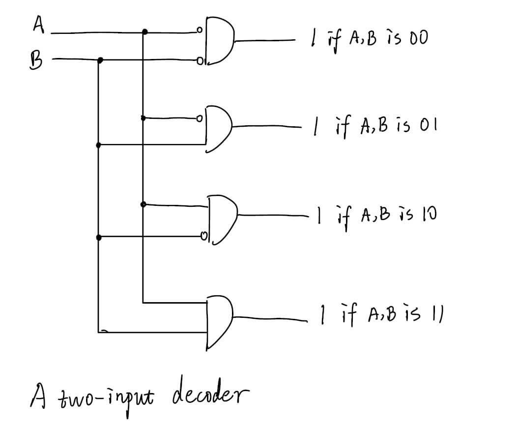
Decoder
A decoder has exactly one input with 1 and the rest are 0s. Which input is 1 is determined by the input pattern.
!
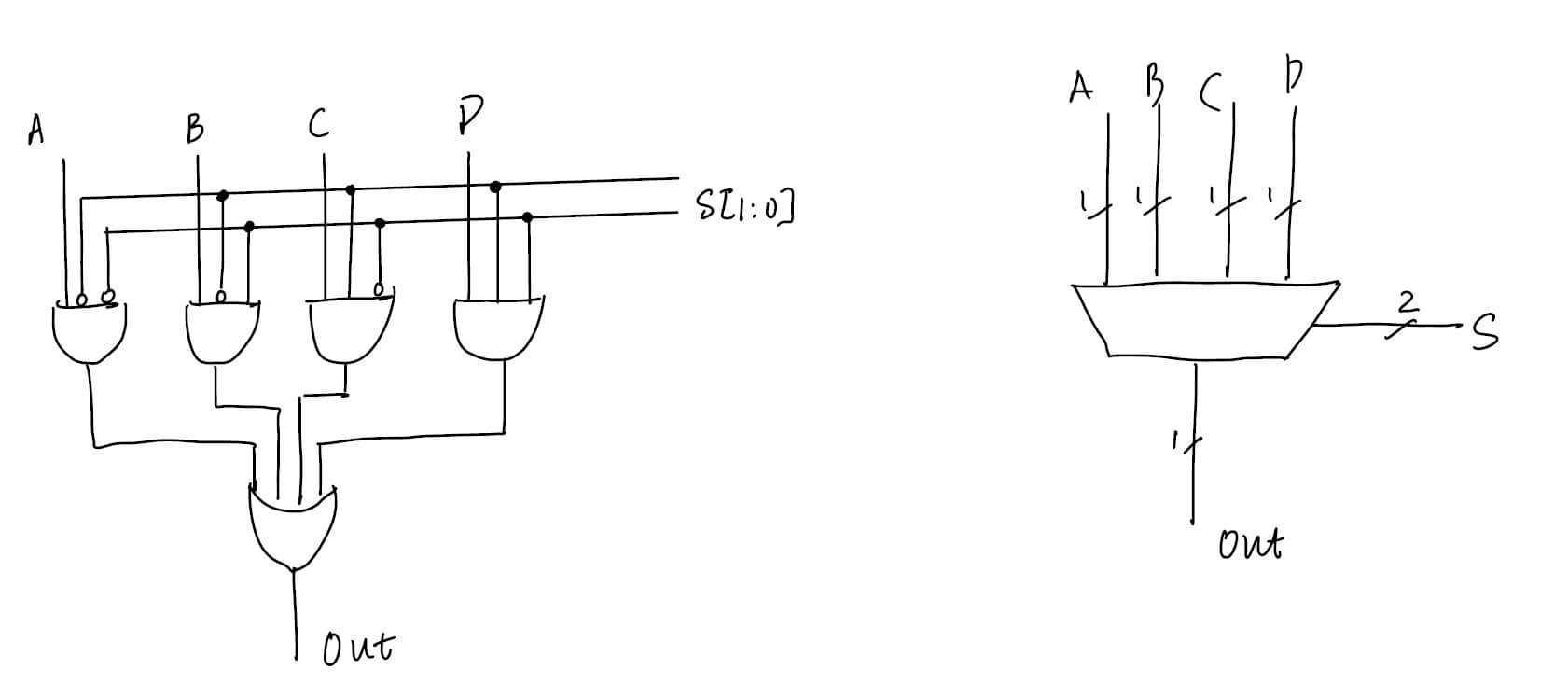
Multiplexer (Mux)
A mux selects one of its inputs and connects it to the output. A mux consists of 2n inputs and n select lines.
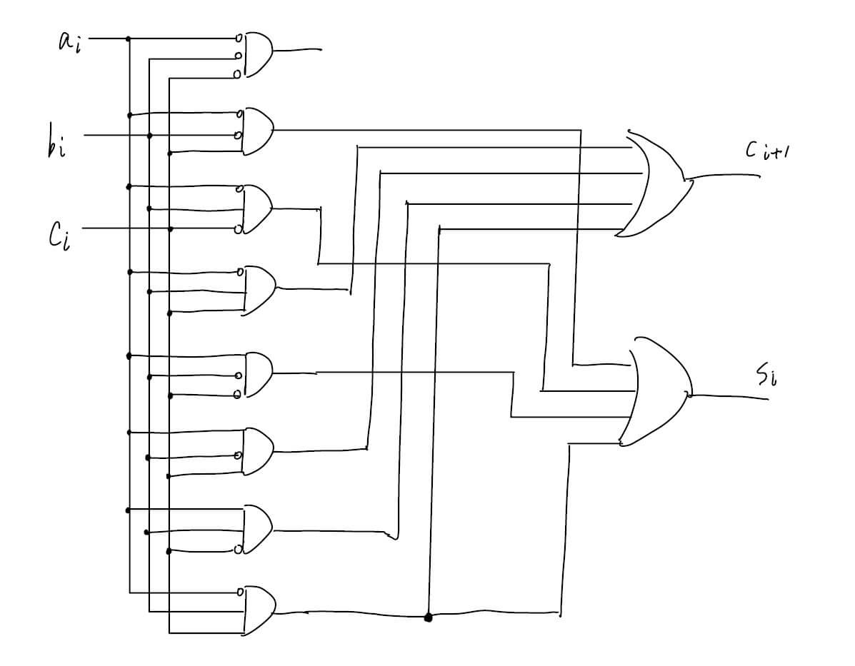
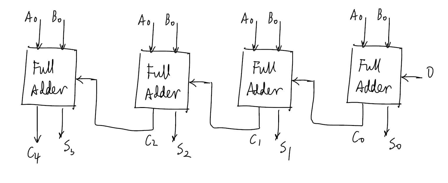
Full Adder
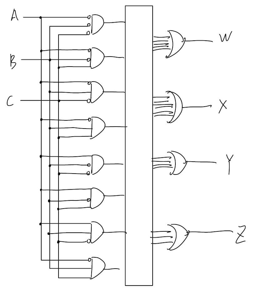
A full adder is an application of the programmable logic array (PLA). Because the set of logic operators {NOT, OR, AND} is logically complete (they can represent any truth table we wish), we use the logic gates {NOT, OR, AND} to implement any logic functions.
The truth table for a full adder is:
| ai | bi | carryi | carryi+1 | si |
|---|---|---|---|---|
| 0 | 0 | 0 | 0 | 0 |
| 0 | 0 | 1 | 0 | 1 |
| 0 | 1 | 0 | 0 | 1 |
| 0 | 1 | 1 | 1 | 0 |
| 1 | 0 | 0 | 0 | 1 |
| 1 | 0 | 1 | 1 | 0 |
| 1 | 1 | 0 | 1 | 0 |
| 1 | 1 | 1 | 1 | 1 |
The circuit for adding two 4-bit binary numbers:
Basic Storage Elements
R-S Latch
Two 2-input NAND gates are connected such that the output of each is connected to one of the inputs of the other.
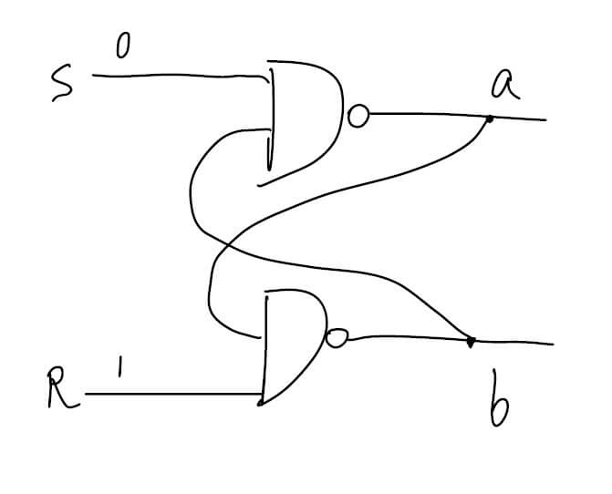
| S | R | a | b | |
|---|---|---|---|---|
| 0 | 0 | - | - | Forbidden |
| 0 | 1 | 1 | 0 | |
| 1 | 0 | 0 | 1 | |
| 1 | 1 | a | b | Quiescent state |
The Gated D Latch
Directly control whether a latch is set/reset by D, when WE (write enable) is asserted.
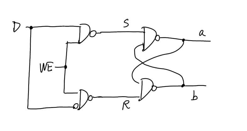
| WE | D | S | R | a | b |
|---|---|---|---|---|---|
| 0 | 0 | 1 | 1 | a | b |
| 0 | 1 | 1 | 1 | a | b |
| 1 | 0 | 1 | 0 | 0 | 1 |
| 1 | 1 | 0 | 1 | 1 | 0 |
Master-slave Flip-flop
A master-slave flip-flop is constructed out of two gated D latches. Suppose the input (1) and output (0) of a master-slave flip-flop is connected through an inverter.
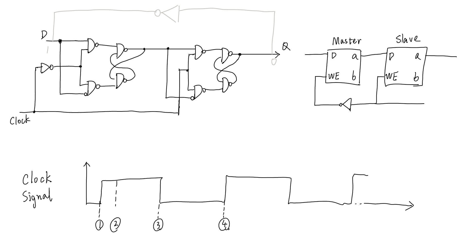
Output (0) is sent to the inverter (at time point 1), which produces 1, and 1 is sent to the input of master (at time point 2). Then, because the clock signal is 1, which means the WE signal of master is 0, it is impossible to change the output of master at this point. Finally, at time point 3, the clock signal is cleared, and the output of master switches to 1, so the master latch can be written, but not the slave latch. At time point 4, the slave latch can finally be written, producing the output (1) and sends it to the inverter.
A register can be constructed with a series of master-slave flip-flops connected to the same clock signal.
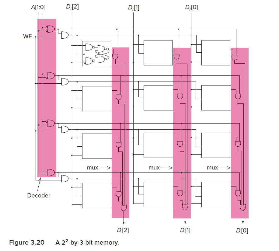
Memory
Address space: the total number of uniquely identifiable locations in the memory.
Addressability: the number of bits stored in each memory location. Most memories are byte-addressable (8 bits).
Word line: each row of memory corresponds to a (typically 8 bit) word.
A 22-by-3-bit memory:
Sequential Logic Circuits
These circuits contain storage elements that keep track of prior history information. The output of a sequential logic circuit depends on both the inputs now and the values stored in the storage elements.
The Concept of State
The state of a system is a snapshot of all the relevant elements of the system at the moemnt the snapshot is taken.
Finite State Machines
A finite state machine consists of:
- A finite number of states
- A finite number of external inputs
- A finite number of external outputs
- An explicit specification of all state transitions
- An explicit specification of what determines each external output
We use a state diagram to represent a finite state machine. A state diagram is a directed graph. Each node represents a state, and each arc represents a valid transition from one state to another. In all our cases, the state transitions depend on the values of external input, and the external output depends solely on the current state (not the input).
The Clock
In electronic circuit implementations of a finite state machine, the transition from one state to another occurs at the start of each clock cycle.
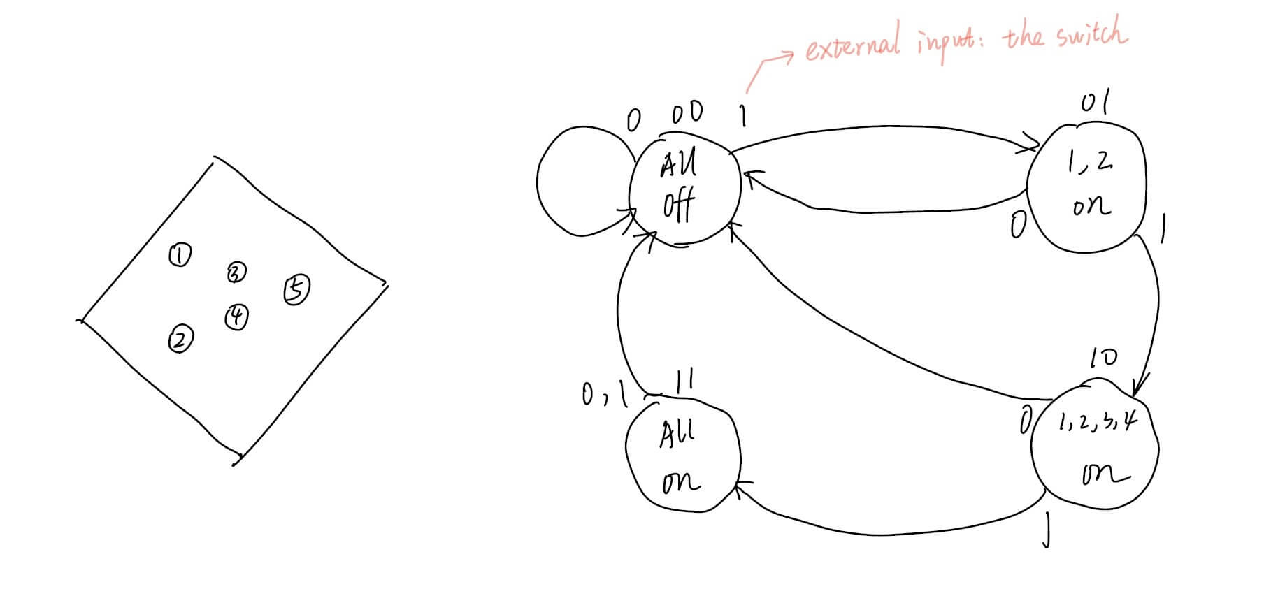
Example: A Traffic Danger Sign
The state diagram of the traffic danger sign controller:
The block diagram:
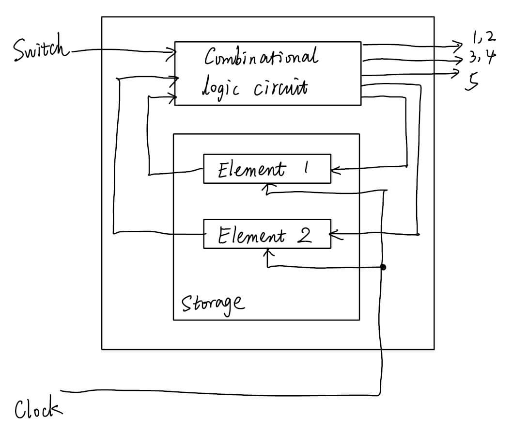
Combinational logic:
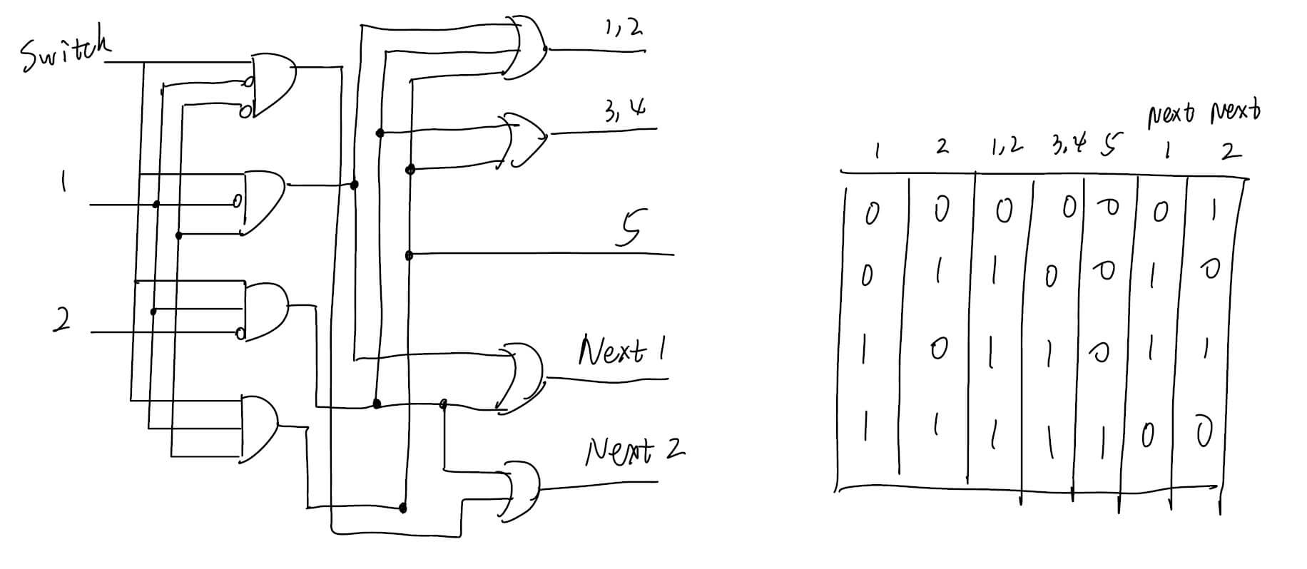
Storage elements: master-slave flip-flop


留下评论
注意 评论系统在中国大陆加载不稳定。