
Chapter 4: The von Neumann Model
Basic Components
Memory
Memory Address Register (MAR): MAR stores the address of the location of memory we want to interrogate.
Memory Data Register (MDR): MDR stores the value we want to read from or write into memory.
Processing Unit
The processing unit carries out the actual processing of information in the computer.
The simplest processing unit is Arithmetic and Logic Unit (ALU). It is capable of executing arithmetic and logic operations. The ALU in LC-3 can perform ADD, AND and NOT functions. These three functions can implement other functions. e.g. a - b = ADD(a, ADD(NOT(b), 1))
Input and Output
Keyboard: Keyboard Data Register (KBDR) holds the ASCII code of keys struck, and Keyboard Status Register (KBSR) holds status information of the keyboard.
Monitor: Display Data Register (DDR) holds the ASCII code of letters to be displayed, and Display Status Register (DSR) holds status of the screen.
Control Unit
It keeps track of where we are in the process of executing the program, and where we are in the process of executing each instruction.
Instruction Register (IR): IR contains the current instruction.
Program Counter (PC): also called instruction pointer. PC stores the memory location of the next instruction to be executed.
Instruction Processing
The Instruction
Opcode: What the instruction does. In LC-3, the opcode takes up 4 bits.
Operands: What to do the instruction to. In LC-3, the opcode takes up 12 bits.
There are three types of instructions in LC-3: operate instructions (which process data), data movement instructions (which move data from one place to another), and control instructions (which change the sequence of instruction execution).
The Instruction Cycle
Instructions are processed under the direction of the control unit in a systematic, step-by-step manner. The sequence of steps is called the instruction cycle. Each step is called a phase. There are 6 phases in an instruction cycle:
Fetch: obtains the next instruction from memory and loads it into IR. It takes multiple steps:
- MAR ← PC, increment PC
- MDR ← M[MAR]. This will take several clock cycles, until MDR is Ready (and a flag named R is set to 1).
- IR ← MDR
Decode: sends the opcode to a 4-to-16 decoder, which identifies the opcode, and decides what to do.
Evaluate address: computes the address of the memory location that is needed to process the instruction. During this step, the processor calculates the memory address to be used, according to the addressing modes specified in the ISA (like adding the offset to PC or Base Register).
Fetch operands: interrogates the memory and obtains the source operands needed to process the instruction.
Execute: carries out the actual execution. For example, performing the addition in the ALU.
Store Result: writes the result in the designated memory destination.
* Testing Interrupt Signal (INT): if INT is asserted, save the current state information in the runtime stack, and load the PC with the starting address of the interrupt routine.
Changing the Sequence of Execution
Control instructions load the PC during the Execute phase, wiping out the incremented PC so that at the start of the next instruction cycle, the processor will get the next instruction from the new PC, not the incremented PC.
Control of the Instruction Cycle
Each phase of every instruction is controlled by the finite state machine of the control unit.
For example, the Fetch phase takes 3 clock cycles. During the first clock cycle, the MAR is loaded with the content of the PC, and the PC is incremented. For this to happen, the finite state machine outputs control signals and asserts GatePC and LD.MAR. It also asserts the select lines of the PCMUX to choose the output of the PC incrementer. We will study the control signals of each phase in each instruction in the next chapter.
Halting the Computer
Stopping the instruction cycle requires stopping the clock. In a computer, the clock signal is produced by a crystal oscillator called the clock generator. Its output is ANDed with the output of the RUN latch. If the RUN latch is in the 1 state (its output is 1), the clock is activated. If the RUN latch is cleared, the clock circuit always outputs 0, thus stopping the clock.
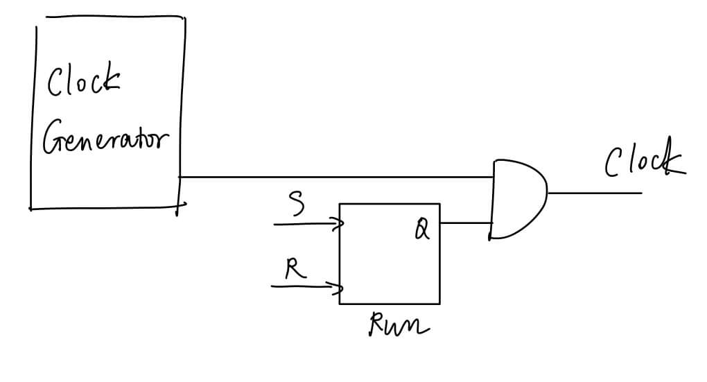
To reinitiate the clock signal, there must be some external mechanism that sets the RUN latch to 1 again.


留下评论
注意 评论系统在中国大陆加载不稳定。