
Chapter 5: The LC-3
The ISA: Overview
Memory Organisation
Address space: 216
Addressability: 16 bits. Because of the size of addressability, we refer to 16 bits as a word.
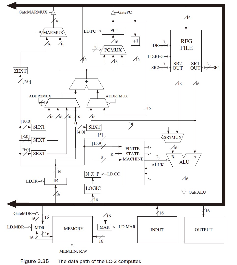
Registers
Unlike memory, which takes multiple clock cycles to access, registers can be accessed in a single machine cycle. In LC-3, each register stores 16 bits of information. There are:
General Purpose Registers (GPR): 8 GPRs in LC-3, labelled R0-R7.
Other registers: they are not directly addressable, but are used and affected by instructions, like the PC and condition codes.
Condition codes are stored in three single-bit registers (N, Z, P) which indicate whether the last result written to the GPR is negative, zero or positive. If the result is negative/zero/positive, the N/Z/P register is set and the other two are cleared.
The Instruction Set
There are 15 opcodes in LC-3. They are:
- Operate instructions: ADD, AND, NOT
- Data movement instructions: LD, LDI, LDR, LEA, ST, STR, STI
- Control instructions: BR, JSR/JSRR, JMP, RTI, TRAP
Data Type
There is only one supported data type in LC-3: 2’s complement integer.
Addressing Modes
LC-3 supports five addressing modes. They are:
- Non-memory addresses: immediate (literal), register
- Memory addresses: PC-relative, indirect, Base+offset
Instructions
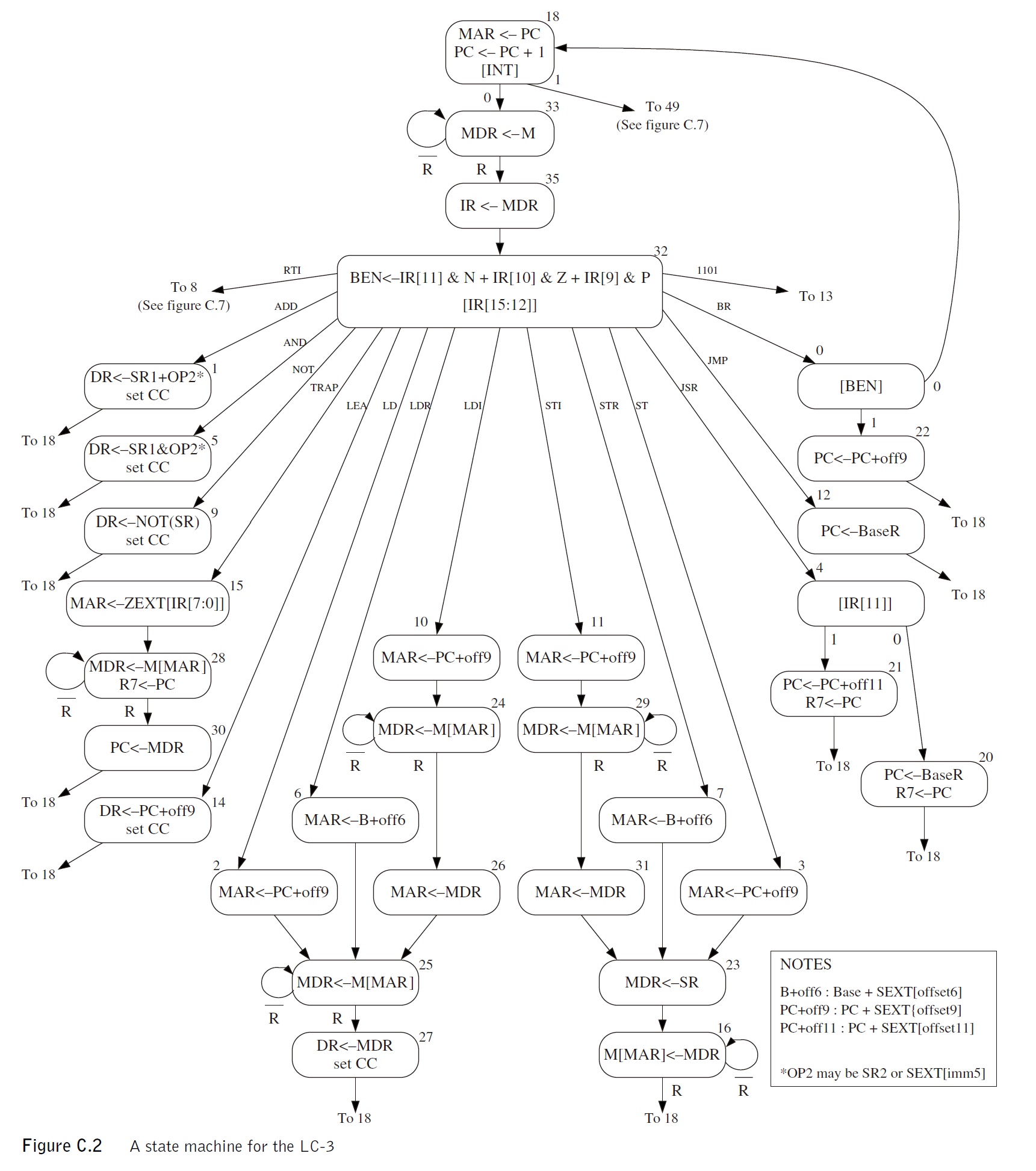
Instruction Fetch Sequence
This sequence takes place at the beginning of the processing of all 16 instructions.
Operation: IR ← M[PC]
| State | RTL | Control Signals |
|---|---|---|
| 18 | MAR ← PC PC <- PC+1 |
GatePC/YES LD.MAR/LOAD LD.PC/LOAD PCMUX selects PC+1 |
| 33 | MDR ← M[MAR] | MEM.EN/YES R.W/RD LD.MDR/LOAD (MDRMUX selects memory [MIO.EN/YES]) (wait for R) |
| 35 | IR ← MDR | GateMDR/YES LD.IR/LOAD |
(RTL stands for Register Transfer Language)
Note: The signal MEM.EN does not come directly from the finite state machine. It is generated by the Address Control Logic. It is asserted when MIO.EN is YES and MAR is other than KBSR, KBDR, DSR or DDR.
Decode Phase
In this phase, the processor decodes the opcode (IR[15:12]) and calculates the BEN (Branch Enable) signal. BEN equals: IR[11] & N + IR[11] & Z + IR[9] & P.
No special control signals are needed here.
Operate Instructions
ADD 0001 Addition
If IR[5] is 0:
Operation: DR ← SR1 + SR2, setcc()
Control signals:
- SR2MUX selects SR2OUT (IR[5]/0)
- ALUK/ADD
- GateALU/YES
- LD.REG/LOAD
- (SR1MUX/8.6)
- (DRMUX/11.9)
- LD.CC/LOAD
If IR[5] is 1:
Operation: DR ← SR1 + SEXT(imm5), setcc()
Control signals:
- SR2MUX selects SEXT (IR[5]/1)
- ALUK/ADD
- GateALU/YES
- LD.REG/LOAD
- (SR1MUX/8.6)
- (DRMUX/11.9)
- LD.CC/LOAD
AND 0101 Bit-wise Logical AND
Very similar to ADD. The only difference is ALUK selects AND.
NOT 1001 Bit-wise Complement
Operation: DR ← NOT(SR), setcc()
Control signals:
- ALUK/NOT
- GateALU/YES
- LD.REG/LOAD
- SR1MUX/8.6
- DRMUX/11.9
- LD.CC/LOAD
Data Movement Instructions
LEA 1110 Load Effective Address (immediate addressing mode)
Operation: DR ← PC + SEXT(PCoffset9), setcc()
Control signals:
- ADDR1MUX/PC
- ADDR2MUX/PCoffset9
- MARMUX/ADDER
- GateMARMUX/YES
- LD.REG/LOAD
- DRMUX/11.9
- LD.CC/LOAD
LD 0010 Load (PC-relative addressing mode)
Operation: DR ← M[PC + SEXT(PCoffset9)], setcc()
| State | RTL | Control Signals |
|---|---|---|
| 2 | MAR ← PC+off9 | ADDR1MUX/PC ADDR2MUX/PCoffset9 MARMUX/ADDER GateMARMUX/YES LD.MAR/LOAD |
| 25 | MDR ← M[MAR] | MEM.EN/YES R.W/RD LD.MDR/LOAD (MDRMUX selects memory) (wait for R) |
| 27 | DR ← MDR, setcc() | GateMDR/YES (DRMUX/11.9) LD.REG/LOAD |
LDI 1010 Load Indirect (Indirect addressing mode)
Operation: DR ← M[M[PC + SEXT(PCoffset9)]], setcc()
| State | RTL | Control Signals |
|---|---|---|
| 10 | MAR ← PC+off9 | ADDR1MUX/PC ADDR2MUX/PCoffset9 MARMUX/ADDER GateMARMUX/YES LD.MAR/LOAD |
| 24 | MDR ← M[MAR] | MEM.EN/YES R.W/RD LD.MDR/LOAD (MDRMUX selects memory) (wait for R) |
| 26 | MAR ← MDR | GateMDR/YES LD.MAR/LOAD |
| 25 | MDR <- M[MAR] | MEM.EN/YES R.W/RD LD.MDR/LOAD (MDRMUX selects memory) (wait for R) |
| 27 | DR < MDR, setcc() | GateMDR/YES (DRMUX/11.9) LD.REG/LOAD |
LDR 0110 Load Base+offset (Base+offset addressing mode)
Operation: DR ← M[BaseR + SEXT(offset6)], setcc()
| State | RTL | Control Signals |
|---|---|---|
| 6 | MAR <- BaseR+off6 | ADDR1MUX/BaseR ADDR2MUX/offset6 MARMUX/ADDER GateMARMUX/YES LD.MAR/LOAD SR1MUX/8.6 |
| 25 | MDR <- M[MAR] | MEM.EN/YES R.W/RD LD.MDR/LOAD (MDRMUX selects memory) (wait for R) |
| 27 | DR < MDR, setcc() | GateMDR/YES (DRMUX/11.9) LD.REG/LOAD |
ST 0011 S (PC-relative addressing mode)
Operation: M[PC + SEXT(PCoffset9)] ← SR, setcc()
| State | RTL | Control Signals |
|---|---|---|
| 3 | MAR ← PC+off9 | ADDR1MUX/PC ADDR2MUX/PCoffset9 MARMUX/ADDER GateMARMUX/YES LD.MAR/LOAD |
| 23 | MDR ← SR | SR1MUX/11.9 ALUK/PASSA GateALU/YES MDRMUX selects bus (MIO.EN/NO) LD.MDR/LOAD |
| 16 | M[MAR] ← MDR | MEM.EN/YES R.W/WR (wait for R) |
STI 1011 Store Indirect (Indirect addressing mode)
Operation: M[M[PC + SEXT(PCoffset9)]] ← SR
| State | RTL | Control Signals |
|---|---|---|
| 11 | MAR ← PC+off9 | ADDR1MUX/PC ADDR2MUX/PCoffset9 MARMUX/ADDER GateMARMUX/YES LD.MAR/LOAD |
| 29 | MDR ← M[MAR] | MEM.EN/YES R.W/RD LD.MDR/LOAD MDRMUX selects memory (MIO.EN/YES) (wait for R) |
| 31 | MAR ← MDR | GateMDR/YES LD.MAR/LOAD |
| 23 | MDR ← SR | SR1MUX/11.9 ALUK/PASSA GateALU/YES MDRMUX selects bus (MIO.EN/NO) LD.MDR/LOAD |
| 16 | M[MAR] ← MDR | MEM.EN/YES R.W/WR (wait for R) |
STR 0111 Load Base+offset (Base+offset addressing mode)
Operation: M[BaseR + SEXT(offset)] ← SR
| State | RTL | Control Signals |
|---|---|---|
| 7 | MAR <- BaseR+off6 | ADDR1MUX/BaseR ADDR2MUX/offset6 MARMUX/ADDER GateMARMUX/YES LD.MAR/LOAD SR1MUX/8.6 |
| 23 | MDR ← SR | SR1MUX/11.9 ALUK/PASSA GateALU/YES MDRMUX selects bus (MIO.EN/NO) LD.MDR/LOAD |
| 16 | M[MAR] ← MDR | MEM.EN/YES R.W/WR (wait for R) |
Control Instructions
JMP / RET 1100 Jump / Return from Subroutine
Operation: PC ← BaseR
Control signals:
- SR1MUX/8.6
- ADDR1MUX/BaseR
- ADDR2MUX/ZERO
- PCMUX/ADDER
- LD.PC/LOAD
Note: RET is a shortcut to JMP R7.
BR 0000 Conditional Branch
First, check BEN (Branch Enabled).
If BEN is 0:
The processor jumps to state 18 and processes the next instruction.
If BEN is 1:
Operation: PC ← PC+off9
Control signals:
- ADDR1MUX/PC
- ADDR2MUX/PCoffset9
- PCMUX/ADDER
- LD.PC/LOAD
JSR / JSRR 0100 Jump to Subroutine
First, check IR[11].
If IR[11] is 1 (JSR):
Operation: PC ← PC+off11, R7 ← PC
Control signals:
- GatePC/YES
- DRMUX/R7
- LD.REG/LOAD
- ADDR1MUX/PC
- ADDR2MUX/PCoffset11
- PCMUX/ADDER
- LD.PC/LOAD
If IR[11] is 0 (JSRR):
Operation: PC ← BaseR, R7 ← PC
Control signals:
- GatePC/YES
- DRMUX/R7
- LD.REG/LOAD
- SR1MUX/8.6
- ADDR1MUX/BaseR
- ADDR2MUX/ZERO
- PCMUX/ADDER
- LD.PC/LOAD
TRAP 1111 System Call
Operation: PC ← M[ZEXT(trapvect8)], R7 ← PC
| State | RTL | Control Signals |
|---|---|---|
| 15 | MAR ← ZEXT[IR[7:0]] | MARMUX/7.0 GateMARMUX/YES LD.MAR/LOAD |
| 28 | MDR ← M[MAR] R7 ← PC |
MEM.EN/YES R.W/RD LD.MDR/LOAD MDRMUX selects memory (MIO.EN/YES) (wait for R) GatePC/YES DRMUX/R7 LD.REG/LOAD |
| 30 | PC ← MDR | GateMDR/YES PCMUX/BUS LD.PC/LOAD |
RTI 1000 Return from Interrupt
Reserved for Chapter 10.


留下评论
注意 评论系统在中国大陆加载不稳定。